
High-Accuracy and Traceable AFM Measurements on Semiconductors and Step Standards: Positioning in Sub-Nanometer Resolution
Atomic force microscopy (AFM) permits surface measurements with highest resolution, even down to atomic levels. It enters dimensions that light microscopes can no longer resolve. This is a noncontact procedure. Forces measured between a very fine measuring tip and the object surface give information about the topography, chemical surface condition, defects, etc. This method is used both in research and in production. Typical areas of application include life science technologies, materials research and semiconductor inspection. Precision is required for positioning measuring tip and sample because only on that way a high spatial resolution is achieved. Piezo-based positioning systems are very good for this scanning method because they not only work with sub-nanometer resolution but also have high dynamics.
Physikalisch-Technische Bundesanstalt (PTB) is presently developing a "low noise metrological AFM" allowing atomic force microscopy to again enter new dimensions. This system will be used for traceable measurements of step standards, which are used for setting other AFM. Quantitative examinations of semiconductor samples to determine critical dimensions, i.e. the smallest structures that can still be reproduced, will also be possible. Depending on the application, two measurement methods are used: Area scan and the so-called Single Point Probing Method.
Two Measurement Methods: Area Scan or Single Point Probing
Using area scan, the AFM tip (as fine as an atom) is excited with constant frequency and amplitude so that it starts to oscillate. Then it is approached to the sample at working distance. The sample is moved under the tip. If the distance varies during scanning, frequency and amplitude of the tip oscillation also change. The position of the sample is corrected in Z axis direction so that the oscillation stays constant. The topography information about the sample surface is then provided by the variation of the Z position together with X and Y coordinates, which are relevant for spatial resolution.
As this area scan, even with highest precision, does not provide enough information about the edges of surfaces with steep structures, another method is used, the "Single Point Probing": Here, the positioning device slowly approaches a recognized step to the tip to measure the step accurately. The direction of motion is the surface normal of the step, i.e. three active axes are required for sample positioning. The characteristic "curve of force", a result of changing frequency, amplitude and phase of the tip oscillation at different parts of the step, is captured. The measurement is repeated at different points, until the entire step has been measured. This measurement method is relatively slow but returns very accurate information about topographically steep areas. It is suitable, for example, also for quantitative measurements on semiconductor structures with very small dimensions from 10 to 20 nm.
The positioning system used for sample scanning has to satisfy high requirements in both measurement methods, in particular with regard to resolution. It must work in the sub-nanometer range because the positioning system used for scanning returns the spatial resolution. At the same time, there are high requirements with regard to dynamics. The faster the scan moves in Z direction, the faster is positioning in X and Y axis direction. This does not only shorten the measuring time but also reduces the drift, which increases during time. Consequently, high dynamics also help achieving better accuracy.
Parallel kinematics
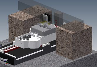
For this reason, PTB decided in favor of a piezo-based nanopositioning system. The parallel kinematics manufactured by market leader PI (Physik Instrumente) is designed for working ranges of 12 µm in three linear axes and works with a resolution of under 0.1 nm. These are the best conditions for it being used in the new AFM. Not only reproducibility is important, but also absolute accuracy, because the AFM is used for quantitative measurements.
This very high motion resolution is only possible because the piezo drives move without classic mechanical components that have friction or mechanical play. The six-axes positioning system has very compact dimensions so that it can perfectly
be fitted in the AFM. On the one hand, it precisely positions the sample in the measurement range, both in X and Y direction and in Z direction. On the other hand, its three rotational axes are used for compensation of parasitic angular errors. This high positioning accuracy is also supported by a high resonant frequency of the overall system of more than 1.4 kHz (with a 300 g load) so that the measurement is not affected by external acoustic interferences.
Sensor technology
For the new atomic force microscope, PTB uses external differential interferometers; they are capable of determining at highest resolution, the motions between the AFM head and the sample on the six-axes positioning system, directly in all six degrees of freedom. With this method, possible disturbing effects, such as drift or elastic warping, between the moving platform of the piezo stage and the sample no longer have an impact, because motions are measured directly by the interferometer; this in return also has a positive effect on the linearity of the AFM measurement. In addition, interferometers provide measurement signals at highest resolution [10 pm] and linearity with a very high dynamic bandwidth.
The interferometer signals are transmitted via a serial data stream to the E-712, a digital controller from PI. This controller can be precisely adapted to the positioning system and features complex error compensation of the six-axes system. The controller provides finely tuned linearization algorithms for an extremely uniform run and fast feed motions with maximum force. By conjointly using parallel kinematics and interferometric measurement of all six degrees of freedom, the E-712 can correct unintended parasitic crosstalk (e.g. caused by external forces) in real time applying corresponding algorithms.
With capacitive sensors, integrated in the piezo stage, a direct position measurement at the position of the AFM head is not possible. But they are important for initialization before the measurement is started:
During initialization, first the absolute-measuring, internal capacitive sensors of the piezo stage are used to approach a defined starting position. Then the servo loop of the piezo stage is closed over external interferometers. They meet PTB standards, but only measure motions and no absolute positions.
With the E-712 digital controller it is also possible to switch between internal (capacitive) and external (interferometric) capture of actual values. This makes high-precision measurements of the surface topology possible.
PTB is positive about the selected solution, and the development of the new AFM is taking place without delay. The advantages of piezo-based drive solutions were convincing, even though the drive that moves the measuring tip to the sample is relatively coarse. The driving force is a so-called PiezoWalk® drive. The NEXLINE drives generate the forward motion by combining longitudinal and shear piezo actuators, i.e. piezo actuators with different motion characteristics. When using specific controls, clamping as well as push motions are possible, which remind of the movement of a quadruped. This drive is used to move the AFM tip to working distance from the sample before the measurement starts. Like this, the AFM tip can be traveled over the entire range of several millimeters with an accuracy of nanometers. After approaching the desired position, the drive has to remain in very stable position so as not to generate additional high-frequency oscillations between the AFM head and the six-axes positioning system; oscillation that cannot be entirely compensated for by the positioning system.
Similar articles
ed.jpg)

More from Physik Instrumente (PI) GmbH & Co. KG
- Individual service for high-end positioning systems 6th February 2018
- Catalogue for alignment of optics and SiP 30th January 2018
- Compact linear stage driven by three-phase linear motor 5th January 2018
- Don't let the shakes ruin your selfie 13th November 2017


Write a comment
No comments