
Testing for electronics material uses microscope stage
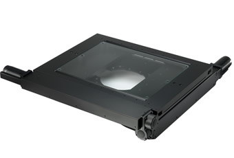
Offering a travel range of over 300x300mm makes the Prior Scientific H112 microscope stage ideal for accurate and precise scanning of semiconductor wafers, photo masks, flat panel displays and printed circuit boards.
Fully compatible with a wide range of microscopes the H112 can easily accommodate wafers up to 300mm (12”) in diameter, or samples up to 25kg in weight, and works with many robot arm wafer loaders. Furthermore, the large (250x250mm) transmitted light area allows transmitted, as well as reflected, light applications to be performed.
The large area scanning capability of the H112 stage is exceptionally precise, with a minimum step size of 0.04µ and a repeatability of +/-0.7µ. The accuracy of the H112 stage, which is enhanced by Prior’s patented Intelligent Scanning Technology (IST), is unmatched. Precision can be further improved with the addition of 100nm encoders for challenging applications requiring the very highest precision.
Prior Scientific microscope stages have a global reputation for top quality and high repeatability. Manufactured using the highest quality components, precision bearings, zero backlash recirculating ball screws, X and Y limit switches, two high precision stepper motors and a tough scratch resistant coating - they provide trouble-free operation over extended periods of time.
Similar articles


More from Prior Scientific Instruments Ltd
- Filter sample holders enhance imaging process 20th January 2017
- Testing for electronics material uses microscope stage 23rd September 2016
- Microscope Stage for Precision Mapping of Large Samples 29th June 2016
- Motorised Z-Axis Microscope Focus Blocks 7th June 2016


Write a comment
No comments